

Ask the Experts: On-site Hydrogen Generation - Secure high purity supply for your critical processes
A steady supply of high-purity hydrogen is critical to semiconductor fabrication. Supply chain interruptions and contamination issues have challenged manufacturers, causing production stoppages. On-site hydroge...
Monitoring Ultra-high Purity Water in Semiconductor Manufacturing
In the fast-evolving world of semiconductors, where single-nanometer linewidths are the new frontier, the role of Ultra-Pure Water (UPW) has never been more critical. In this webinar, you will gain insights fro...
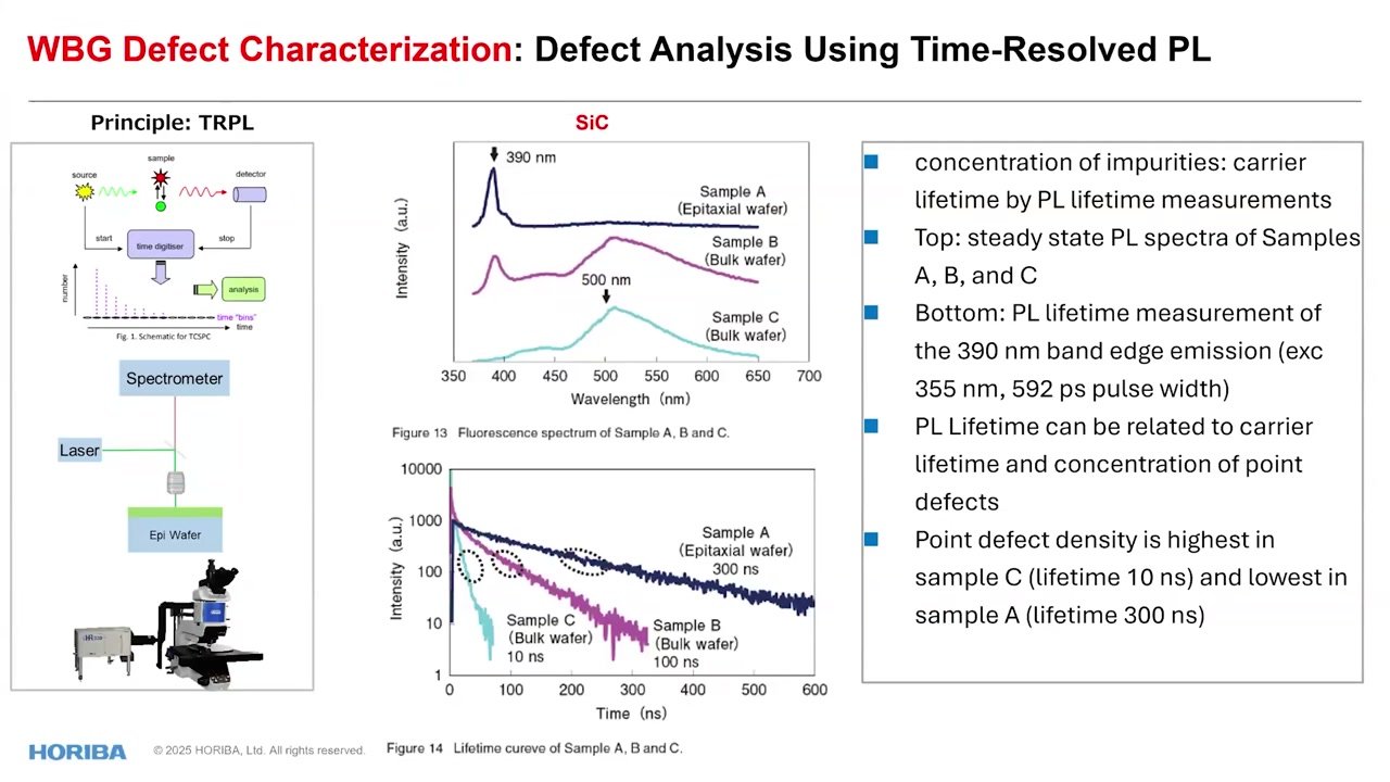
Spectroscopic Characterization of Yield-killing Defects in Wide Bandgap Semiconductor Wafers
Wide bandgap semiconductors such as SiC, GaN, and diamond are critical materials for next-generation power electronics, optoelectronics, and quantum technologies. However, their performance is highly sensitive ...
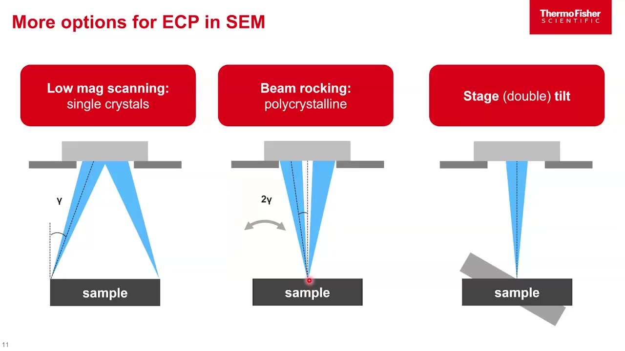
Optimizing Yield: Crystalline defect metrology in III-V materials for microelectronics applications
Requirements for crystalline defect analysis have increased with the introduction of compound semiconductors in electronics applications. Characterization of crystalline defects during epitaxial growth optimiza...
Advancing full wafer and compound semiconductor research with Raman & PL imaging
Semiconductors are the materials from which the engines of the information age are built, and their advancement is among the most vital endeavours in technology. The first step in their production generally inv...
Advancements in Ultrapure Hydrogen Generation for Semiconductor Manufacturing
The CHIPS & Science Act, along with evolving domestic content regulations for electric vehicles and charging infrastructure subsidies, continues to drive significant investment in semiconductor fabrication ...
|
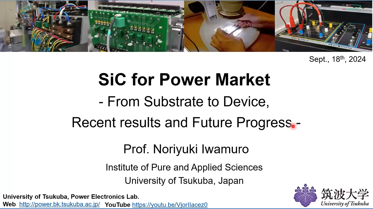
SiC for power market: from substrate to device, recent results and future progress.
SiC has superior efficiency to (Si) IGBT in the high voltage (600-3,300V) space and the high current (several hundred amperes) field that is in the spotlight in relation to EVs. SiC MOSFETS issues to be solved ...

Sample preparation and TEM imaging techniques for advanced power devices
Compound semiconductors, like SiC and GaN, are increasingly attractive for their ability to operate at higher voltages, currents, and frequencies, especially in power and RF devices. However, fabricating wafers...

Multimodal Characterization of Wide Bandgap Semiconductor Wafers
There are many factors that affect wafer yield such as uniformity and defectivity amongst others. Currently optical spectroscopies such as Raman and Photoluminescence are some of the techniques of choice in ass...
Considerations for Thin Film Deposition in Compound Semiconductor Manufacturing
Compound semiconductor materials are used in a wide range of current and emerging applications including LEDs, laser diodes, IR detectors, RF filters, RF power amplifiers, supercomputing and quantum dots. These...


Copyright © 2025 • Angel Business Communications Ltd.