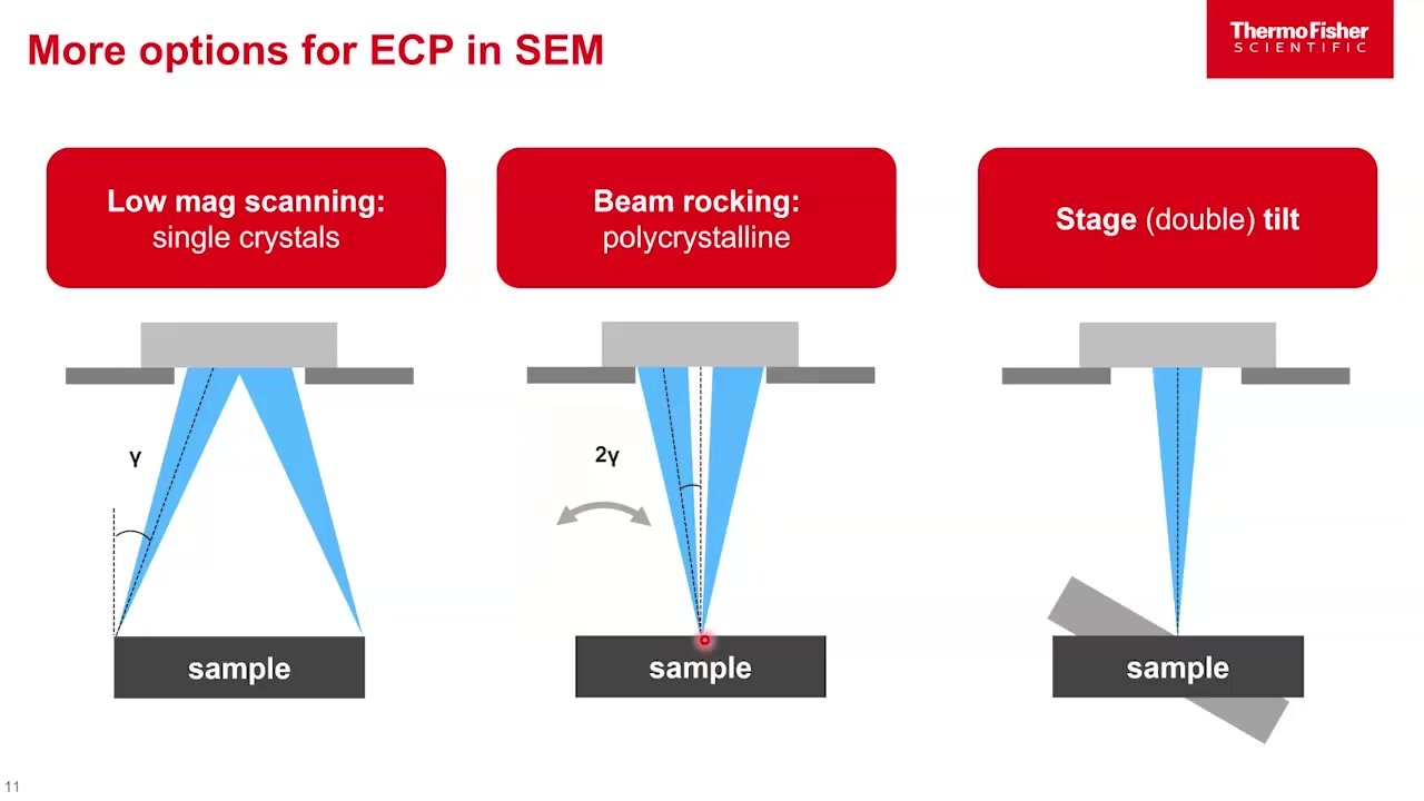
Optimizing Yield: Crystalline defect metrology in III-V materials for microelectronics applications
Requirements for crystalline defect analysis have increased with the introduction of compound semiconductors in electronics applications. Characterization of crystalline defects during epitaxial growth optimiza...
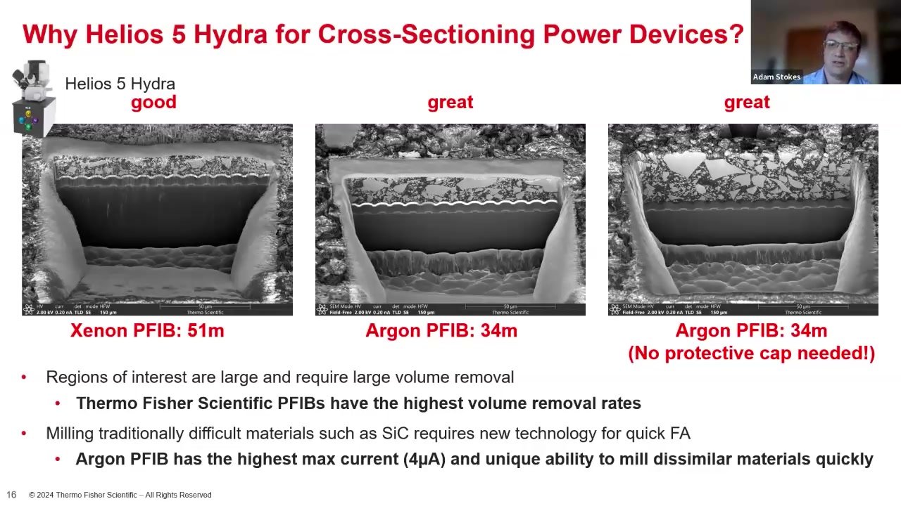
Sample preparation and TEM imaging techniques for advanced power devices
Compound semiconductors, like SiC and GaN, are increasingly attractive for their ability to operate at higher voltages, currents, and frequencies, especially in power and RF devices. However, fabricating wafers...


Copyright © 2025 • Angel Business Communications Ltd.