


|
The Apple Revenue Opportunity MSPs Are Leaving on the Table: What Top-Performing Practices Are Doing Differently in 2026
Most MSPs are sitting on an untapped Apple revenue opportunity and don't know it. In this session, Sophie Milburn and Tim Cruz break down where the money is being left on the table, why it happens, and what top...
Patching That Keeps Users Productive: Best Practices for Smooth IT Operations
When we talk about patching, the focus is often on fixing security vulnerabilities or adding new functionality to operating systems and third-party applications. However, patching policies that fail to consider...
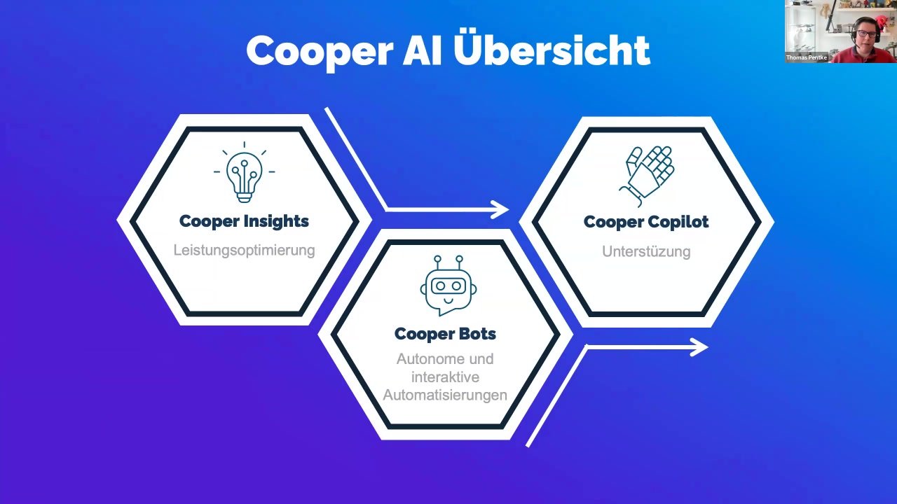
KI-Automatisierung für MSPs: Effizienter Arbeiten, Höhere Margen
Entdecken Sie, wie führende MSPs mit KI-Automatisierung bis zu 30 % mehr Effizienz und höhere Margen erzielen – in einer praxisnahen Live-Session mit Kaseya-Experte Thomas Pentke. Erleben Sie, w...
|
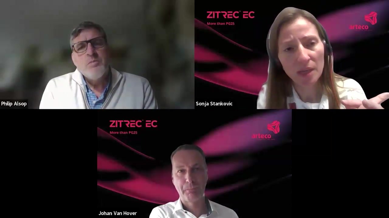
ECO COOLANTS for data centers: reduced product carbon footprint while maintaining quality and performance
Arteco, a global leader in liquid cooling solutions, announces the launch of its ECO product line for the data center industry. To address the growing challenges driven by the unprecedented demand for compute ...
Silicon Photonics Optical Circuit Switches: Adapting Data Centers to AI Workloads
AI and data megatrends are driving explosive growth in computing demands, pushing the limits of current infrastructure. Traditional copper-based scale-up networks and rigid scale-out architectures are becoming ...
Ask the Experts: On-site Hydrogen Generation - Secure high purity supply for your critical processes
A steady supply of high-purity hydrogen is critical to semiconductor fabrication. Supply chain interruptions and contamination issues have challenged manufacturers, causing production stoppages. On-site hydroge...
Precision Motion Solutions for Advanced Packaging: Accelerating Hybrid Bonding & TGV Drilling
Learn how Aerotech's advanced motion control systems and laser processing capabilities address the demanding requirements of emerging advanced packaging technologies. We'll explore how our solutions enable sub-...
Ask the experts - track busway - the future of data centre power distribution?
In today's fast-evolving data center landscape, power infrastructure is under immense pressure to keep up with rising AI workloads, high-density computing, and the need for greater efficiency. Traditional power...

Exascale Connectivity: Building the Neural Networks of AI Infrastructure
Join us on this journey to uncover how embracing cutting-edge technologies and fostering industry collaboration can empower AI to achieve its full, world-changing potential. This webinar, hosted by AFL's Manja...
Monitoring Ultra-high Purity Water in Semiconductor Manufacturing
In the fast-evolving world of semiconductors, where single-nanometer linewidths are the new frontier, the role of Ultra-Pure Water (UPW) has never been more critical. In this webinar, you will gain insights fro...

Delivering a Maintenance-Free Feedback Solution with Battery-less Energy Harvesting Encoder
Presenting energy harvesting technology and highlighting Broadcom´s AS20-M42M series absolute encoder: Battery-less multi-turn counter integrated to a magnetic single-turn ASIC. The innovative solution is...
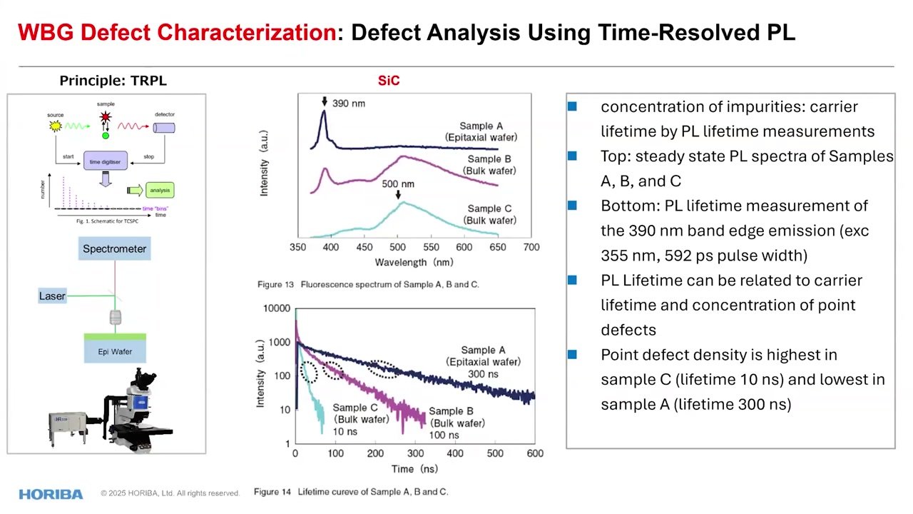
Spectroscopic Characterization of Yield-killing Defects in Wide Bandgap Semiconductor Wafers
Wide bandgap semiconductors such as SiC, GaN, and diamond are critical materials for next-generation power electronics, optoelectronics, and quantum technologies. However, their performance is highly sensitive ...
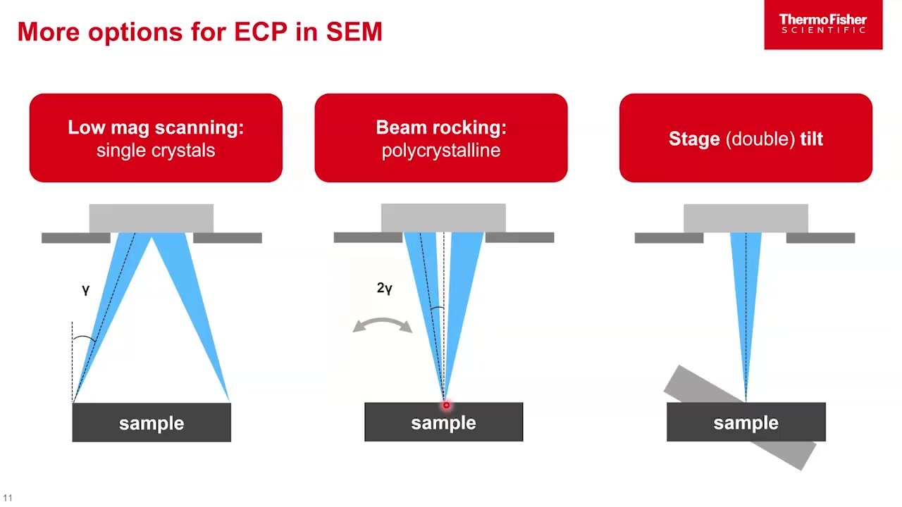
Optimizing Yield: Crystalline defect metrology in III-V materials for microelectronics applications
Requirements for crystalline defect analysis have increased with the introduction of compound semiconductors in electronics applications. Characterization of crystalline defects during epitaxial growth optimiza...

Modeling and Optimizing PICs for Datacenter Interconnects
Datacenter traffic is growing exponentially, driven by demanding applications like AI/ML Training, Cloud Computing, and Video Streaming. Photonic integrated circuits (PICs) have become an enabling technology in...

Advancing full wafer and compound semiconductor research with Raman & PL imaging
Semiconductors are the materials from which the engines of the information age are built, and their advancement is among the most vital endeavours in technology. The first step in their production generally inv...
Advancements in Ultrapure Hydrogen Generation for Semiconductor Manufacturing
The CHIPS & Science Act, along with evolving domestic content regulations for electric vehicles and charging infrastructure subsidies, continues to drive significant investment in semiconductor fabrication ...

Broadcom's Industrial Time-of-Flight Sensor Solutions
The AFBR-S50 optical sensor modules are multi-pixel distance and motion measurement devices based on the indirect Time-of-Flight (iTOF) principle. In this webinar we will present the Broadcom® AFBR-S50 TOF-sen...
|
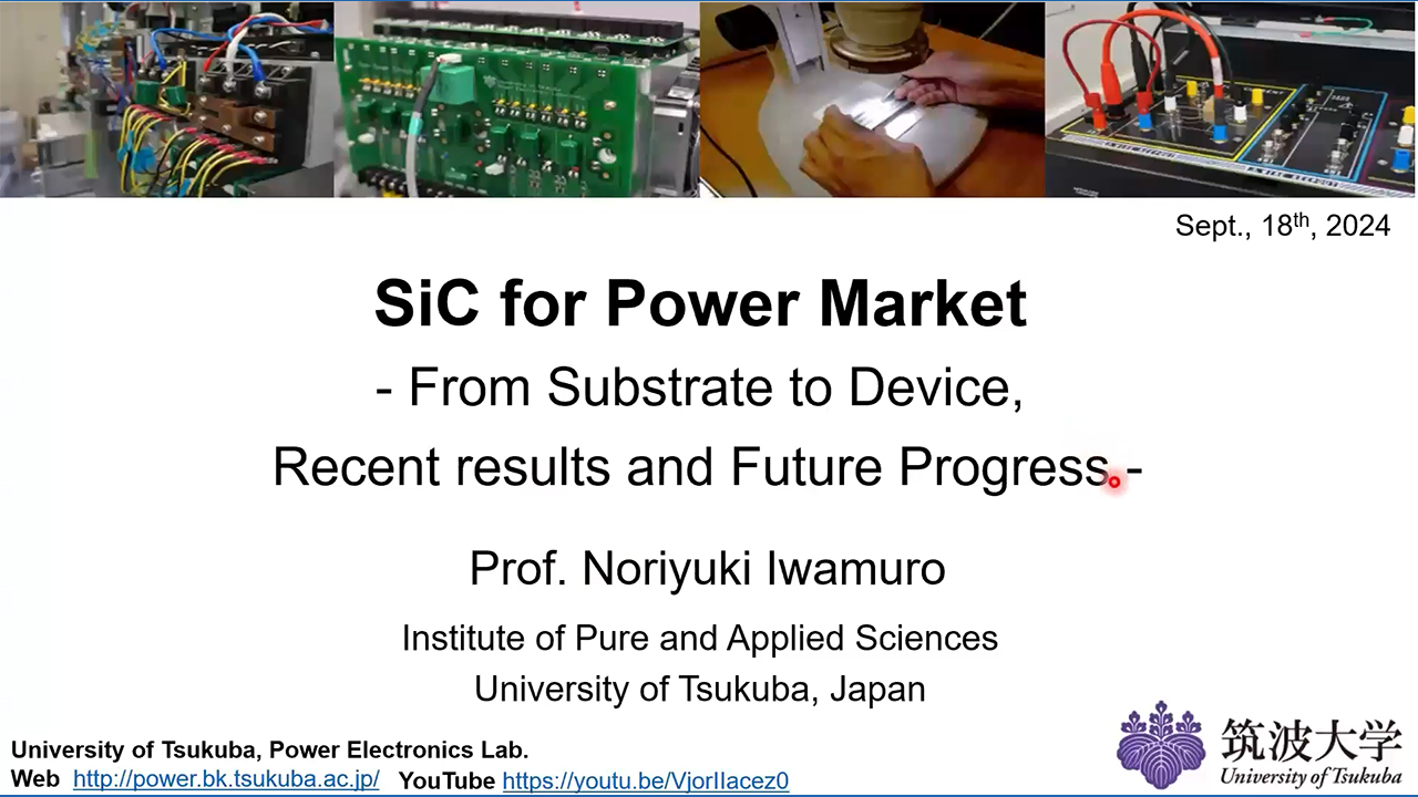
SiC for power market: from substrate to device, recent results and future progress.
SiC has superior efficiency to (Si) IGBT in the high voltage (600-3,300V) space and the high current (several hundred amperes) field that is in the spotlight in relation to EVs. SiC MOSFETS issues to be solved ...

AIOPS-focused roundtable event: Know Before You Go
Whether you choose to call this ecosystem Hybrid Digital Infrastructure Management or Digital Operations Management, there is no doubt that AIOPS has a major role to play in a digital business.Find out how AIOP...
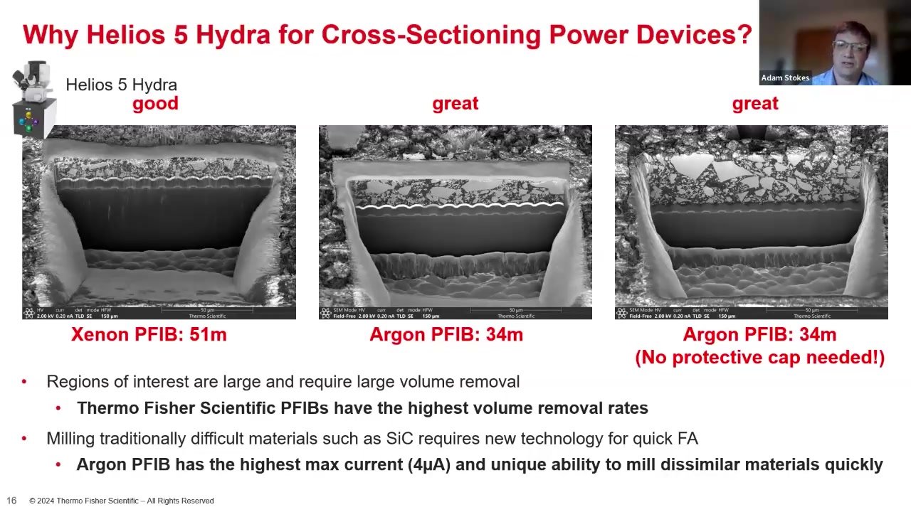
Sample preparation and TEM imaging techniques for advanced power devices
Compound semiconductors, like SiC and GaN, are increasingly attractive for their ability to operate at higher voltages, currents, and frequencies, especially in power and RF devices. However, fabricating wafers...
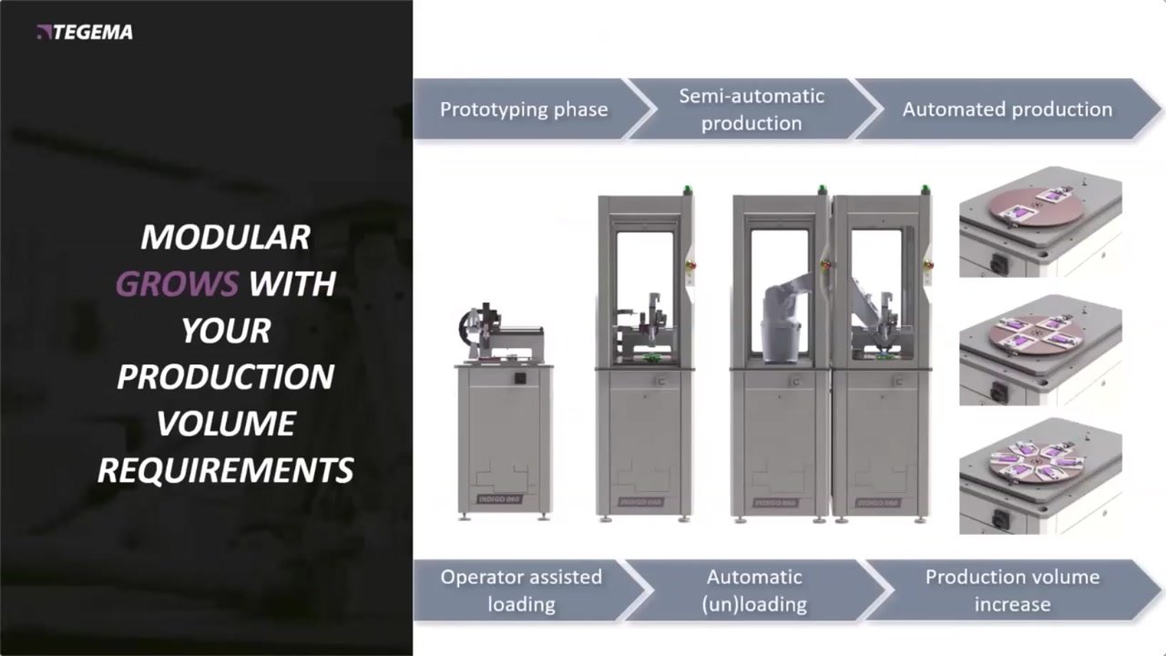
Assembly and Packaging of Photonic Integrated Circuits: A Modular Concept Towards a Fully Automated Process
Physik Instrumente and Tegema hosted a live webinar in association with PIC Magazine, focusing on Assembly and Packaging of Photonic Integrated Circuits. Part One - Modular Machine Platform Enables Breakthrou...
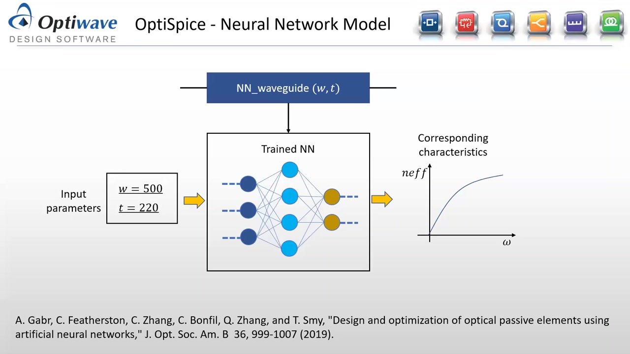
PIC circuit optimization using compact models with physical parameters
In this webinar, photonic integrated circuit design, simulation, and optimization will be demonstrated using 3rd party EDA tools combined with Optiwave software.Building fab-based photonic design kit components...
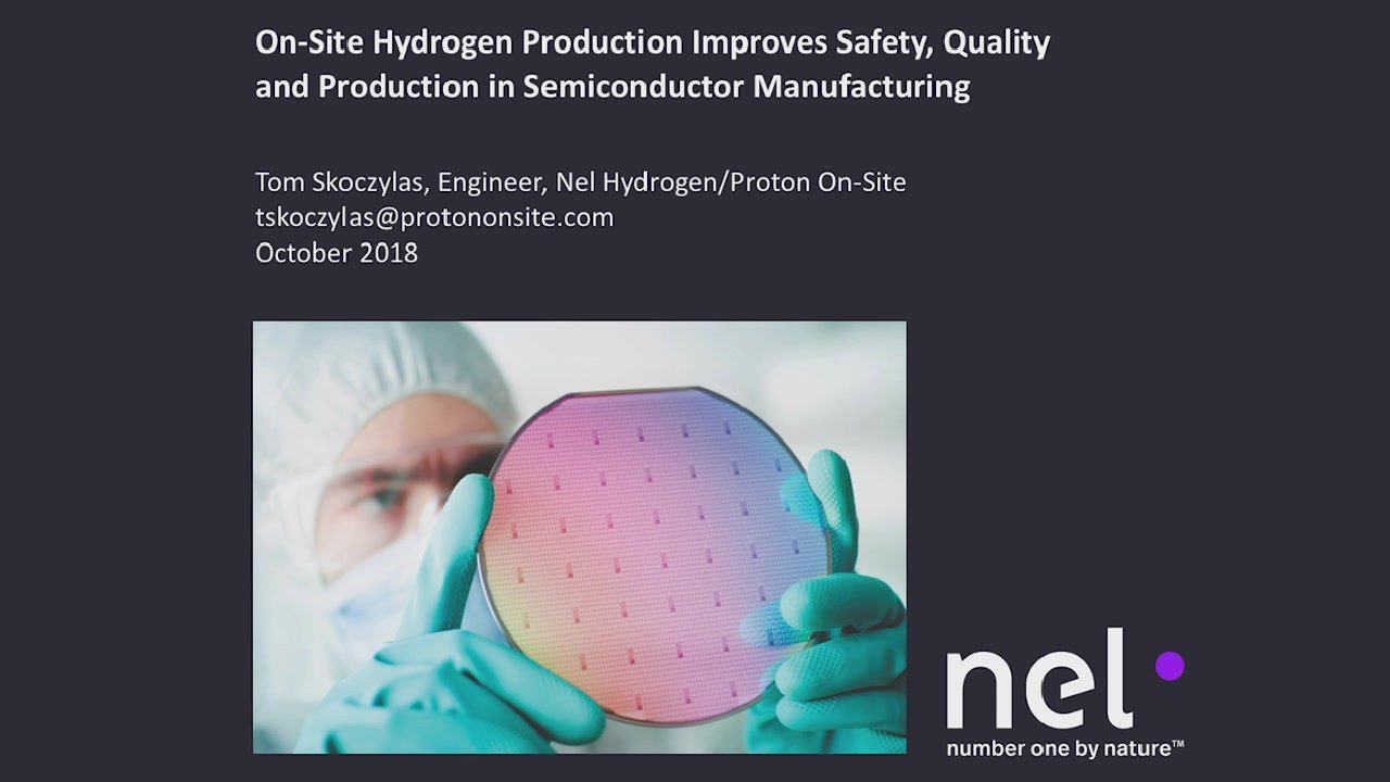
On-Site Hydrogen Production Improves Safety, Quality, and Productivity in Wafer, Chip and Semiconductor Manufacturing
The webinar, presented by Tom Skoczylas in USA & Europe and by Luc Zhu, Chief Representative in China will cover Annealing, Epitaxy, Deposition, Stabilizing, and Lithography, includes a 20 minute Live Q&A sessi...

Say goodbye to traditional storage and hello to a new server based, cloud-managed approach
Be one of the first to learn about this revolutionary approach, which gives enterprises an alternative to restrictive & expensive storage solutions with an API first approach to storage.Cloud-defined storag...
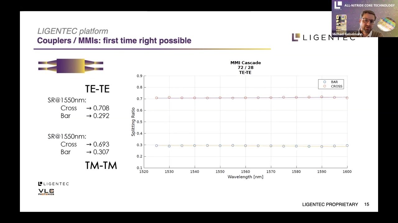
Low Loss SiN PIC Fabrication with LIGENTEC
LIGENTEC is your manufacturing partner for low loss silicon nitride photonic integrated circuits. Our customers benefit from a clear path to volume production while obtaining also small quantities of wafers wit...

The Winds of Change; Unlock the Power of Airflow Management in the Data Center
A must-attend webinar for data center professionals aiming to safely raise operating temperatures, boost performance, reduce airflow leakage, and slash costs.In this session, you'll uncover the secrets of optim...

Multimodal Characterization of Wide Bandgap Semiconductor Wafers
There are many factors that affect wafer yield such as uniformity and defectivity amongst others. Currently optical spectroscopies such as Raman and Photoluminescence are some of the techniques of choice in ass...

Water scarcity - an impending semiconductor crisis?
An individual fab can use tens of millions of gallons of water per day, the equivalent to the daily household water consumption of a small city (population 122,000).Grundfos experts will discuss how today’s t...
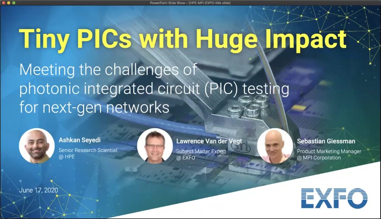
Tiny PICs with Huge Impact: Meeting the Challenges of Photonic Integrated Circuits testing for next-generation networks
In this webinar, discover how the collaborative EXFO, HPE, and MPI PIC testing solution addresses market challenges, making wafer testing faster, scalable, and more reliable, ultimately improving speed-to-marke...
Smart Manufacturing in the Subfab
This webinar will show how successful subfab strategies are not grounded in the technology of Smart Manufacturing alone, but are based around a holistic focus on machines, people, and business process that deli...
Considerations for Thin Film Deposition in Compound Semiconductor Manufacturing
Compound semiconductor materials are used in a wide range of current and emerging applications including LEDs, laser diodes, IR detectors, RF filters, RF power amplifiers, supercomputing and quantum dots. These...
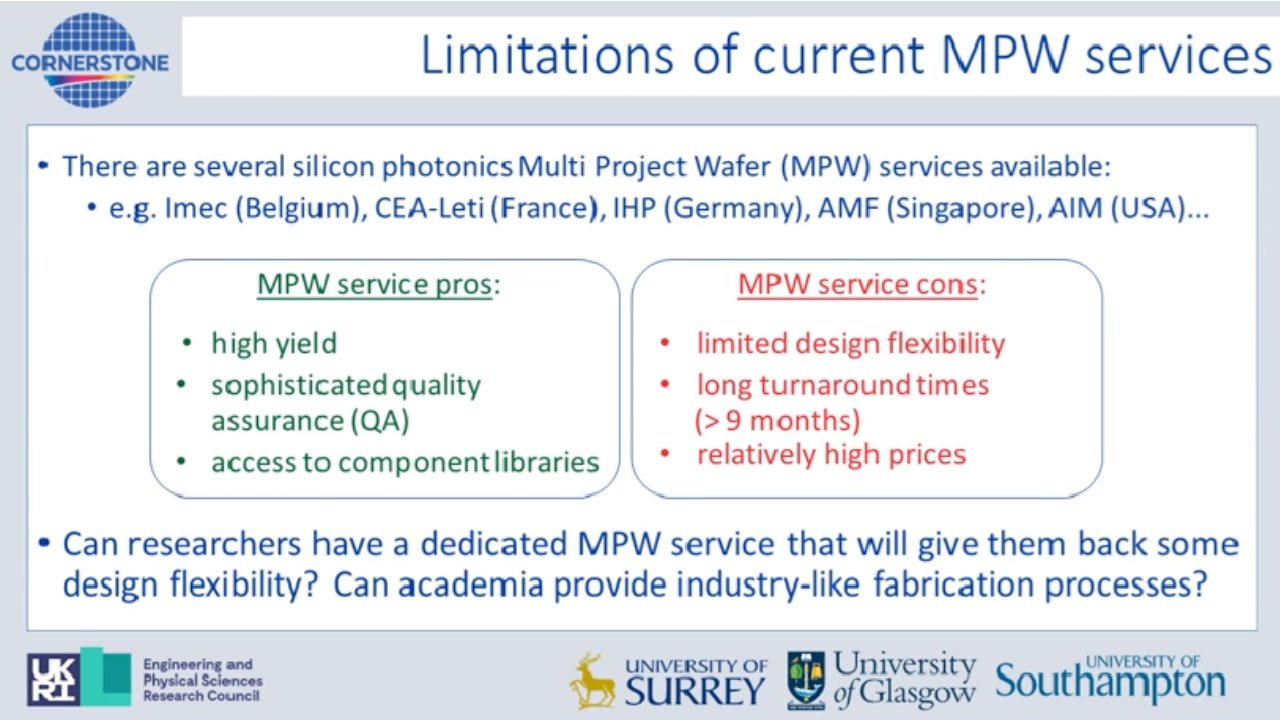
Versatile SiP fabrication with CORNERSTONE
Explores key advantages in Silicon Photonics fabrication through the CORNERSTONE programme at the University of Southampton, UK. Introducing us to CORNERSTONE is Graham Reed - Professor of Silicon Photonics at ...


Copyright © 2025 • Angel Business Communications Ltd.